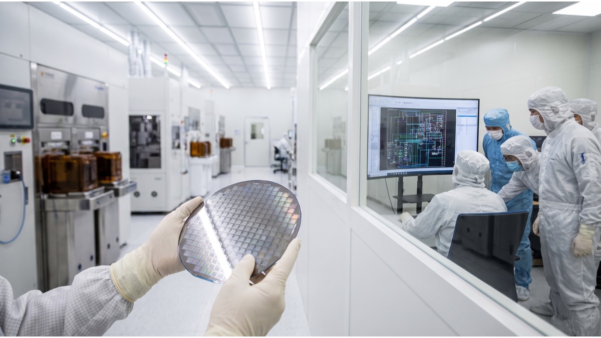
Every time a new flagship smartphone launches, most of the public conversation focuses on the camera, the screen, or the price. But the component doing the most technical heavy lifting — and consuming the largest share of the phone's research and development budget — is the system-on-chip, or SoC, the single piece of silicon that packs together the processor, graphics engine, memory controllers, and increasingly a dedicated AI accelerator. Understanding how that chip actually comes into existence explains a lot about why phones improve the way they do each year, and why a chip announced today won't appear in a device for a long time afterward. It also explains why the handful of companies capable of designing and manufacturing these chips wield outsized influence over the entire smartphone industry, well beyond what their public visibility as brand names might suggest.
The path from a blank engineering whiteboard to a working chip inside a device sold at retail involves several genuinely distinct disciplines: circuit architecture, physical layout automation, semiconductor fabrication, rigorous testing, and advanced packaging, each staffed by different specialists using different tools and facing different constraints. A delay or breakthrough at any single stage can shift the entire timeline, and understanding each stage individually makes it much easier to follow why the smartphone chip industry moves the way it does, why certain companies dominate certain stages, and why genuinely disruptive changes in this space are comparatively rare.
It Starts With Architecture, Years Before Silicon
The process of designing a smartphone chip begins long before any physical manufacturing, in a phase called architecture design. Engineers decide how many processor cores the chip will have, how those cores will be divided between high-performance and high-efficiency roles, how much cache memory sits at each level, and how the graphics and AI processing blocks will communicate with the rest of the system. These decisions are made using extensive simulation software rather than physical prototypes, since building and testing a real chip for every design option would be prohibitively slow and expensive.
This architectural stage typically takes one to two years on its own, and the decisions made here lock in tradeoffs that can't easily be reversed later. A chip optimized heavily for raw processing speed, for instance, tends to run hotter and drain battery faster, while a chip optimized for efficiency may sacrifice peak performance in demanding tasks like gaming or video editing. Chipmakers spend enormous effort trying to strike a balance that fits the specific way people actually use their phones, which is part of why companies invest so heavily in usage-pattern research before finalizing an architecture.
A related architectural decision involves how many distinct processor core types to include and in what proportions, an approach often described as a heterogeneous or big.LITTLE-style design. Rather than building a chip with several identical cores, most modern smartphone SoCs mix a small number of high-performance cores meant for short, demanding bursts of activity with a larger number of smaller, more efficient cores meant to handle the constant low-level background tasks a phone performs even while sitting idle in a pocket. Software running on the phone, coordinated by the operating system, then decides moment to moment which type of core should handle a given task, a balancing act that has become increasingly sophisticated as chips have added more distinct core types rather than fewer.
Turning a Design Into a Physical Layout
Once the architecture is settled, engineers translate it into a physical layout — an extraordinarily detailed blueprint describing the exact position of billions of individual transistors and the microscopic wiring connecting them. This stage, called physical design, is where abstract engineering decisions become a literal map of silicon geography, and it's almost entirely computer-automated because no team of humans could manually place billions of components with the required precision.
A critical part of physical design is deciding which manufacturing process, or 'node,' the chip will be built on. Process nodes are typically described by a number of nanometers, and a smaller number generally means transistors are packed more densely, which tends to improve both performance and power efficiency. Moving to a smaller node isn't simply a matter of shrinking the existing design, though — it usually requires substantial redesign work to account for how electrical behavior changes at that scale, which is one reason smartphone chip generations don't always arrive on a perfectly predictable yearly schedule.
Fabrication: Where Silicon Becomes a Chip
Fabrication is the physical manufacturing stage, carried out in specialized facilities called foundries that represent some of the most capital-intensive industrial infrastructure in the world, often costing tens of billions of dollars to build a single advanced facility. Only a small handful of companies globally operate foundries capable of manufacturing the most advanced smartphone chips, which is why most major chip designers don't own their own factories and instead contract out fabrication to these specialized foundry companies.
The fabrication process itself involves repeatedly layering, etching, and doping ultra-thin films onto a silicon wafer using techniques like photolithography, where patterns are projected onto the wafer using precisely controlled light, sometimes at wavelengths so specific that the machines involved are among the most complex pieces of equipment ever built. A single advanced smartphone chip can require hundreds of individual processing steps, and the entire fabrication run for one batch of chips can take several months from start to finish.
Testing, Yield, and Why Not Every Chip Is Identical
After fabrication, every chip on a wafer goes through extensive testing before it's ever installed in a device, since manufacturing defects at this scale of precision are common enough that a meaningful percentage of chips on any given wafer simply won't work correctly. The percentage of chips that pass testing is called yield, and improving yield is one of the most closely watched metrics in the entire chip industry, since even small yield improvements translate into significant cost savings at the scale of millions of units.
Chips that pass testing but don't quite meet the top performance specification aren't necessarily discarded — they're often sold as a lower-tier variant with some cores or features disabled, a practice called binning. This is part of why a chip family sometimes includes several versions with slightly different core counts or clock speeds, even though they may have started as physically identical silicon that simply performed differently during testing.
Packaging: Connecting the Chip to the Rest of the Phone
Once individual chips are cut from the wafer, they go through packaging, where the raw silicon die is encased and connected to the electrical contacts that will eventually link it to the rest of the phone's circuitry. Modern smartphone chips increasingly use advanced packaging techniques that stack multiple silicon components, such as the processor and memory, extremely close together in three dimensions rather than laying them out flat, which reduces the physical distance data has to travel and improves both speed and power efficiency.
This packaging stage has become an increasingly important area of innovation in its own right, since the physical limits of shrinking transistors further are becoming harder and more expensive to push against. Some of the most significant performance gains in recent chip generations have come not from smaller transistors alone, but from smarter packaging that lets different components work together more efficiently.
Who Actually Designs These Chips
A relatively small number of companies design the chips that power the overwhelming majority of the world's smartphones, and their business models differ in an important way. Some companies design chips exclusively for their own devices, tightly integrating the silicon with their own operating system and software so that hardware and software teams can optimize for each other directly, a process that generally allows for deeper customization but requires an enormous in-house engineering organization to pull off.
Other companies design chips specifically to sell to a wide range of phone manufacturers, competing on the open market for design wins across many different brands and price tiers. This second model requires balancing the needs of many different customers at once, from budget phones to flagships, and tends to produce chips with broader, more general-purpose capability rather than features narrowly tuned to a single company's product line. Both approaches have proven commercially viable, and the competition between them is a major driver of the pace of improvement across the industry as a whole.
Underlying nearly all of these designs, regardless of which company sells the finished chip, is a shared foundation of processor instruction-set architecture licensed from specialized architecture companies, which supply the fundamental blueprint that individual chip designers then customize, extend, and optimize according to their own priorities.
The Rise of Dedicated AI Processing Blocks
Until relatively recently, a smartphone chip's general-purpose processor cores handled essentially all computing tasks, including the kind of pattern-recognition workloads now associated with on-device artificial intelligence features like photo enhancement, voice recognition, and predictive text. General-purpose cores can technically run these workloads, but they do so inefficiently compared to hardware built specifically for the kind of repetitive mathematical operations that machine learning models rely on.
In response, chipmakers began adding a dedicated block to the chip specifically optimized for these AI-style calculations, often called a neural processing unit or similarly branded term depending on the manufacturer. This dedicated hardware can complete certain AI-related tasks using a small fraction of the power a general-purpose core would need for the same task, which matters enormously in a battery-powered device where every fraction of a watt affects how long the phone lasts between charges.
As on-device AI features have expanded from simple photo processing to more complex tasks like real-time translation and generative content creation, the amount of chip area and design effort devoted to this dedicated AI hardware has grown substantially with each generation, to the point where it now represents one of the primary areas competing chip designers use to differentiate their products from one another.
Security Features Built Directly Into the Silicon
Modern smartphone chips also carry substantial responsibility for security, well beyond what most users ever directly see. A dedicated, physically isolated region of the chip, often called a secure enclave or secure element depending on the manufacturer, is specifically designed to store and process highly sensitive information like fingerprint data, facial recognition templates, and cryptographic keys used for payments, keeping this data walled off from the rest of the operating system even if other parts of the phone's software are compromised.
This hardware-level isolation exists because software-only security measures can potentially be bypassed if an attacker gains sufficiently deep access to the operating system, whereas physically separating the most sensitive operations onto dedicated silicon adds a meaningfully harder barrier to overcome. Chip-level security has become an increasingly prominent design priority as phones have taken on more responsibility for financial transactions, digital identity, and access to increasingly sensitive personal data.
This is also why chipmakers now dedicate specific engineering teams solely to security architecture, distinct from the teams working on raw performance or efficiency, reflecting how much the priorities of chip design have broadened beyond simply making the processor faster from one generation to the next.
Why Chip Development Costs Shape Phone Prices
Designing a leading-edge smartphone chip has become extraordinarily expensive, with the combined cost of architecture, physical design, and the specialized software tools needed to manage billions of transistors now running into the hundreds of millions of dollars for a single generation, before a single unit has been fabricated. Advanced fabrication itself adds further cost on top of that, since manufacturing on the most modern process nodes requires access to some of the most expensive industrial equipment ever built, and foundries pass a share of that capital cost on to their customers through the price charged per finished chip.
These costs are only recoverable if a chip sells in enormous volume, which is part of why only a handful of companies compete seriously at the very top of the smartphone chip market, and why entering that market from scratch as a new competitor has become almost prohibitively difficult. It also explains a pattern consumers can observe directly: flagship phones using the newest, most advanced chips tend to command the highest prices, while phones built on chips from a slightly older generation, or manufactured on a less cutting-edge process node, are able to reach noticeably lower price points, since much of the enormous upfront design and tooling cost has already been recovered by the time that chip is used in a more budget-oriented device.
Why the Whole Cycle Takes Years
Counting from initial architecture planning to a finished chip shipping inside a retail smartphone, the full cycle typically spans two to three years, which is why chip roadmaps are planned so far in advance and why a delay at any single stage, from a fabrication issue to a packaging bottleneck, can ripple forward into delayed product launches many months later.
This long lead time also explains why chip companies and phone manufacturers work on next-generation designs while the current generation is still being sold — by the time a flagship phone reaches store shelves, engineering teams are typically already deep into the architecture and physical design of chips that won't appear in a shipping product for another one to two years.
It also means that the specific chip powering whatever flagship phone is generating headlines today was, in a very real sense, designed for a version of the market that existed two or three years earlier, based on assumptions about camera technology, display technology, and typical app workloads that engineers had to guess at well before those trends were fully clear, which is part of why chip design teams invest so heavily in forecasting rather than simply reacting to the present.
Why Yield Determines Everything
Not every chip on a wafer works, since microscopic defects are unavoidable at these dimensions, and the proportion that functions is called yield.
Yield drives cost far more than the price of raw silicon, because a wafer costs roughly the same to process regardless of how many working chips it produces.
This is why larger chips are disproportionately expensive, since a bigger area is more likely to contain a defect, and it is a substantial reason designs are split into smaller pieces.
How Binning Turns Defects Into Products
Chips that fail testing at full specification are frequently still usable at lower clock speeds or with defective sections disabled entirely.
Manufacturers sell these as lower-tier products, which means a budget chip is often physically identical to a premium one with parts switched off.
This practice, called binning, converts what would otherwise be waste into revenue, and it explains why product ranges frequently share an underlying design.
The chip inside a smartphone represents years of layered engineering decisions, from abstract architectural tradeoffs made long before any physical silicon exists, through automated physical design, capital-intensive fabrication, careful testing and binning, increasingly sophisticated packaging, dedicated AI hardware, and hardware-level security. Each generation's improvements come from advances across all of these stages working together rather than any single breakthrough, which is part of why year-over-year gains have become more incremental even as the underlying engineering effort keeps growing. For consumers, the practical takeaway is that a chip's marketing name and headline speed figures capture only a small slice of what actually went into it. The real story spans design teams working years ahead of a product's release, foundries operating some of the most sophisticated industrial equipment ever built, and increasingly a race to fit specialized AI and security hardware onto the same small piece of silicon — all coordinated across a global supply chain that few other consumer products depend on as heavily. That same complexity is also why the smartphone chip industry remains concentrated among so few companies, and why disruptions anywhere along this chain, from a shortage of a specific manufacturing material to a delay at a single advanced foundry, can ripple outward to affect phone availability and pricing worldwide months later. The next time a new phone's chip is announced, it's worth remembering that what's being unveiled publicly is really the final, visible step of a process that started years earlier and touched dozens of specialized engineering disciplines along the way, most of which never appear in a single keynote slide or marketing spec sheet, yet quietly determine whether that phone actually lives up to what was promised on stage during the launch event.
Sources
- Wikipedia — overview of system-on-chip design and components
- IEEE Spectrum — technical coverage of semiconductor design and fabrication
- Taiwan Semiconductor Manufacturing Company (TSMC) — background on foundry fabrication processes from a leading chip manufacturer
- Arm — background on mobile processor architecture licensing
- IEEE International Electron Devices Meeting — academic and industry research on semiconductor device technology
FAQ
How long does it take to design and manufacture a smartphone chip?
The full cycle from initial architecture planning to a finished chip shipping in a retail phone typically takes two to three years.
Why do most chip designers not own their own factories?
Building and operating an advanced chip fabrication facility can cost tens of billions of dollars, so most chip designers contract manufacturing out to specialized foundry companies instead.
What does 'binning' mean in chip manufacturing?
Binning is the practice of selling chips that pass testing but don't meet top performance specifications as lower-tier variants with some features or cores disabled, rather than discarding them.
Does a smaller process node number always mean a better chip?
Generally smaller nodes improve performance and efficiency by packing transistors more densely, but moving to a smaller node requires substantial redesign and doesn't automatically guarantee better real-world performance on its own.
Why do chip generations sometimes arrive later than expected?
Because the process involves many sequential stages, a delay at any single stage, from fabrication issues to packaging bottlenecks, can push back the entire timeline to a shipping product.
About the Author
We reference Wikipedia, IEEE Spectrum, Taiwan Semiconductor Manufacturing Company (TSMC), Arm, and IEEE International Electron Devices Meeting to explain the background and current understanding of this topic.
Loved This Article?
Share it on WhatsApp → Share it on WhatsApp
Get more guides in your inbox — Subscribe to our newsletter for weekly surprising stories from Egypt, Saudi Arabia, Dubai, and beyond.