A single grain of dust would ruin it. A speck of dirt a fraction the width of a human hair could destroy features being built at a scale smaller than a virus. And yet, from that starting point of near-impossible precision, factories around the world reliably produce chips containing tens of billions of individual transistors, each one working correctly, billions of times a second, for years on end. Understanding how that is actually achieved reveals one of the most extraordinary manufacturing processes humans have ever built.
This matters well beyond technical curiosity. Chip fabrication capacity has become a matter of national economic strategy and geopolitical importance, the physical scale being etched has become so small that it now bumps against the limits of physics itself, and the extraordinary cost of building a modern factory explains why only a handful of companies on Earth can compete at the cutting edge at all.
Why Chip Factories Are Called Fabs
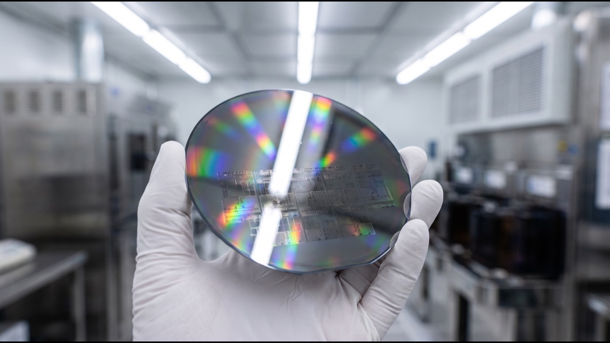
A chip manufacturing facility is commonly called a fab, short for fabrication plant, and it bears almost no resemblance to a conventional factory. Rather than assembly lines of visible parts being bolted together, a fab is a sequence of extraordinarily precise chemical, optical, and physical processes applied repeatedly to a thin circular disc of silicon called a wafer.
A single wafer, typically around 300 millimeters across today, does not produce just one chip. It is processed to contain hundreds of identical chip patterns simultaneously, printed side by side across its surface, which are only separated into individual chips at the very end of the manufacturing process.
The entire process, from a bare, unprocessed wafer to a finished chip ready for testing, can involve many hundreds of individual processing steps and take several weeks to complete, even though the finished product is a piece of silicon smaller than a fingernail.
It Starts With Sand: Making the Silicon Wafer
Silicon, the base material for the overwhelming majority of chips, is derived from ordinary sand, specifically silicon dioxide, which is refined through an intensive chemical process into extraordinarily pure silicon, with purity levels reaching roughly 99.9999999 percent, a level of chemical purity almost unmatched by any other manufactured material.
That purified silicon is melted and grown into a large cylindrical crystal called an ingot, using a process that carefully controls the crystal structure as it solidifies, since chip performance depends on the silicon's atomic structure being extremely uniform and free of defects across the entire cylinder.
The finished ingot is sliced into thin, mirror-polished discs called wafers, each just under a millimeter thick, which then become the base material onto which every subsequent manufacturing step is applied. A single ingot can yield many wafers, each destined to become hundreds of individual chips.
Why the Clean Room Has to Be So Extreme
Every stage of chip fabrication after this point happens inside a clean room, an environment engineered to remove airborne particles to a degree that dwarfs anything found in a hospital operating theater. Leading-edge fabs maintain particle counts thousands of times lower than an ordinary room, filtering air continuously through multiple stages of extremely fine filtration.
This extreme cleanliness is necessary because the circuit features being built on a modern chip are measured in nanometers, smaller than most bacteria and comparable in scale to many viruses. A single dust particle, invisible to the naked eye, landing on a wafer during a critical step can permanently short-circuit or break a feature, destroying every chip in that immediate area of the wafer.
Workers inside a fab wear full-body clean suits, commonly nicknamed bunny suits, covering essentially every part of the body, since human skin, hair, and even breath shed particles constantly. Air pressure inside the cleanest zones is kept higher than surrounding areas specifically so that air always flows outward through any opening, preventing contaminated air from drifting in.
Photolithography: Printing Circuits With Light
The core process that actually creates a chip's circuit pattern is called photolithography, and it works somewhat like an extraordinarily precise photographic printing process. A light-sensitive chemical coating is applied evenly across the wafer surface, and then light is projected through a patterned mask, or reticle, that contains the design of one layer of the chip's circuitry.
Where light passes through the mask and strikes the coating, a chemical reaction occurs that changes how that coating responds to subsequent processing, effectively transferring the circuit pattern from the mask onto the wafer's surface with extraordinary precision, repeated hundreds of times across the wafer to print the same pattern onto every individual chip site simultaneously.
A modern chip requires dozens of distinct lithography steps, each printing a different layer of the circuit design precisely aligned on top of the previous layers, with alignment tolerances measured in mere nanometers, since even a tiny misalignment between layers can render the resulting circuit non-functional.
What EUV Actually Changed
For decades, lithography used deep ultraviolet light at a specific wavelength, but as chip designers pushed circuit features smaller and smaller, that wavelength of light eventually became too large relative to the features being printed, similar to trying to paint extremely fine detail with an increasingly blunt brush.
Extreme ultraviolet lithography, commonly called EUV, solved this by using light at a vastly shorter wavelength, allowing dramatically finer circuit features to be printed directly. Generating that specific wavelength of light reliably at industrial scale required decades of dedicated research and remains one of the most technically demanding engineering achievements in modern manufacturing.
EUV light is absorbed by essentially all materials, including air itself, which means the entire optical path from light source to wafer must operate inside a near-perfect vacuum, using mirrors instead of conventional lenses since no known material can efficiently transmit EUV light through it, adding enormous additional engineering complexity to an already extraordinarily precise process.
Etching, Doping, and Building Up Layers
After lithography defines a pattern on the light-sensitive coating, etching processes remove material from the exposed areas, carving the actual circuit pattern permanently into the silicon or into thin material layers deposited on top of it, using precisely controlled chemical or plasma-based processes.
Doping is a separate but equally essential process, where specific impurity atoms are deliberately introduced into precise regions of the silicon to change its electrical properties, creating the fundamental building blocks, called transistors, that switch electrical current on and off to perform logical operations.
A modern chip is built up as dozens of extremely thin layers stacked on top of each other, alternating between depositing new material, patterning it with lithography, etching it into shape, and sometimes doping it, repeated in careful sequence until the complete three-dimensional structure of the chip's circuitry is complete.
Why Modern Chips Are Built in 3D
Transistors were historically built as flat, two-dimensional structures laid across the silicon surface, but as engineers pushed transistor sizes smaller, purely flat designs began suffering from electrical leakage that degraded performance and wasted power, since the physical channel controlling current flow had become too small to control reliably in a flat geometry.
Modern transistor designs instead build vertical, three-dimensional structures, allowing the controlling gate to wrap more completely around the current-carrying channel, dramatically improving how tightly current flow can be controlled even at extremely small physical dimensions, extending the industry's ability to keep shrinking transistors well past where flat designs would have stalled.
This three-dimensional approach adds considerable manufacturing complexity, requiring extraordinarily precise etching and deposition steps to build genuinely vertical structures reliably across an entire wafer, but it has become essential to sustaining the decades-long trend of packing more transistors into the same physical chip area.
Testing the Wafer Before It Is Even Cut
Before a finished wafer is cut into individual chips, it undergoes electrical testing while still whole, using an array of extremely fine probes that make contact with each individual chip site on the wafer surface and run a battery of electrical tests to identify which sites are functioning correctly.
This wafer-level testing allows manufacturers to map exactly which chip locations on the wafer are defective before investing further time and cost in cutting, packaging, and finishing them, since discovering a defect at this early stage is far cheaper than discovering it after a chip has already been fully packaged.
The resulting wafer map also feeds directly into yield analysis, helping engineers identify whether defects cluster in particular patterns, which can reveal a specific equipment problem or process drift that needs correcting before it affects an even larger number of wafers.
Dicing, Packaging, and Final Testing
Once testing identifies which chip sites are functional, the wafer is cut, or diced, into individual chips using an extremely precise saw or, increasingly, a laser-based cutting process, separating what was one continuous piece of silicon into hundreds of separate, physically identical chips.
Each functional chip is then packaged, meaning it is mounted onto a small substrate and enclosed in protective material, with tiny wires or solder connections linking the chip's microscopic internal circuitry to the external pins or contacts that will eventually connect it to a circuit board inside a phone, computer, or other device.
Packaged chips undergo a further round of final testing, checking performance, power consumption, and reliability under a range of conditions, sometimes including deliberately stressing chips at elevated temperatures to identify units that might fail early, before they are sorted, binned by performance level, and shipped to device manufacturers.
Why Chip Yields Are Never 100 Percent
Given the extraordinary precision required across hundreds of manufacturing steps, some proportion of chips on every wafer will always be defective, a reality manufacturers describe using the term yield, meaning the percentage of chips on a wafer that function correctly and meet performance specifications.
Yield naturally starts low whenever a manufacturer introduces a new, smaller manufacturing process, since the process itself is still being refined, and gradually improves over months as engineers identify and correct sources of defects, a maturation curve that is closely watched throughout the semiconductor industry as an indicator of how successfully a new manufacturing generation is progressing.
Chips that fail testing at the highest performance tier are frequently not discarded entirely but instead sold as lower-performance variants with certain features disabled, a practice called binning, which allows manufacturers to extract commercial value from imperfect but still partially functional silicon rather than wasting it.
Why a Fab Costs Tens of Billions of Dollars
A single leading-edge fabrication plant today can cost tens of billions of dollars to build and equip, a figure driven overwhelmingly by the cost of the extraordinarily specialized equipment inside it, with individual EUV lithography machines alone costing well over one hundred million dollars each, and a single fab requiring dozens of such tools working in careful coordination.
Beyond equipment cost, the facility itself must be engineered to extraordinary tolerances, including vibration isolation precise enough that a truck driving past outside could otherwise disrupt nanometer-scale alignment, along with power, water purification, and chemical handling infrastructure built to a scale and reliability standard far beyond conventional industrial construction.
These enormous fixed costs must be recovered across the volume of chips a fab can produce over its operating life, which is precisely why leading-edge semiconductor manufacturing has consolidated into an industry structure with only a small number of companies capable of sustaining that level of continuous capital investment.
Why So Few Companies Can Do This
The combination of extreme capital cost, deep specialized engineering expertise accumulated over decades, and the need to continuously invest in the next generation of even more precise manufacturing technology has narrowed the field of companies operating at the leading edge of chip fabrication to a genuinely small number worldwide.
This concentration has significant strategic implications, since a large share of the world's most advanced computing capability, from smartphones to artificial intelligence systems to modern military equipment, ultimately depends on manufacturing capacity concentrated in a small number of facilities operated by an even smaller number of companies.
Governments around the world have responded to this concentration with substantial subsidies and incentives aimed at building or expanding domestic fabrication capacity, recognizing that the extraordinary manufacturing process described here has become not just a commercial matter but a genuine question of national economic and strategic resilience.
This same logic increasingly shapes investment decisions in the Gulf region as well, where governments have begun courting chip designers, packaging facilities, and data-center operators as part of broader economic diversification strategies, recognizing that even capturing a share of the value chain surrounding fabrication, rather than leading-edge fabrication itself, carries meaningful long-term economic value.
The equipment supply chain feeding into fabrication is itself remarkably concentrated, with a small number of specialized companies supplying critical tools like lithography systems, deposition equipment, and the ultra-pure chemicals consumed throughout the process, meaning a disruption at any single link in that chain can ripple through chip production worldwide within weeks.
Every phone, laptop, car, and data center in daily use ultimately traces back to this same extraordinary sequence: purified sand, grown into a crystal, sliced into wafers, patterned with light finer than a wavelength most people will never see, etched, doped, tested, cut, and packaged, hundreds of times over, inside some of the most precisely controlled environments humans have ever built.
Sources
- Wikipedia — overview of semiconductor fabrication processes
- Intel — technical documentation on chip manufacturing and process technology
- TSMC — foundry documentation on lithography and fabrication processes
- U.S. National Institute of Standards and Technology — semiconductor measurement and manufacturing standards
- Semiconductor Industry Association — industry data on fabrication capacity and investment
FAQ
Why do chip factories need to be so extraordinarily clean?
Because the features being etched are smaller than most airborne dust particles, so a single stray particle landing on a wafer can permanently ruin an entire chip.
What does EUV lithography actually stand for and do?
Extreme ultraviolet lithography uses an extremely short wavelength of light to etch far smaller circuit features onto silicon than older lithography methods can achieve.
Why does chip manufacturing cost so much money?
A single modern fabrication plant can cost tens of billions of dollars, driven mainly by the price of extreme-precision equipment like EUV lithography machines and the ultra-clean facilities that house them.
Why do only a handful of companies operate leading-edge chip factories?
The capital cost and technical difficulty of building and operating a leading-edge fabrication plant are so extreme that only a small number of companies worldwide can sustain the investment.
What happens to a chip design after it leaves the fab?
Finished wafers are cut into individual chips, tested, and packaged into the protective casing with external connectors before being shipped to device manufacturers.
About the Author
We reference Wikipedia, Intel, TSMC, the U.S. National Institute of Standards and Technology, and the Semiconductor Industry Association to explain the background and current understanding of this topic.
Loved This Article?
Share it on WhatsApp → Share it on WhatsApp
Get more guides in your inbox — Subscribe to our newsletter for weekly surprising stories from Egypt, Saudi Arabia, Dubai, and beyond.