A modern smartphone chip packs tens of billions of transistors onto a piece of silicon smaller than a fingernail, each one built with precision measured in individual atoms. Getting there starts with ordinary sand and ends inside facilities that count among the most complex and expensive industrial sites humans have ever built.
The process explains not just how a chip actually gets made, but why a single new factory can cost tens of billions of dollars, why only a handful of companies on Earth can produce the most advanced chips, and why a shortage at one facility can ripple through car factories and phone manufacturers worldwide.
What a Chip Actually Is at the Physical Level
A computer chip is fundamentally a thin slice of silicon etched with an intricate network of microscopic switches called transistors, wired together into circuits that perform the logical operations underlying every calculation a computer or phone ever carries out.
The sophistication lies almost entirely in scale and precision rather than in the underlying concept, since a single modern processor chip can contain tens of billions of these switches, each one built to dimensions measured in mere nanometers.
Why Chip Manufacturing Requires Extraordinary Cleanliness
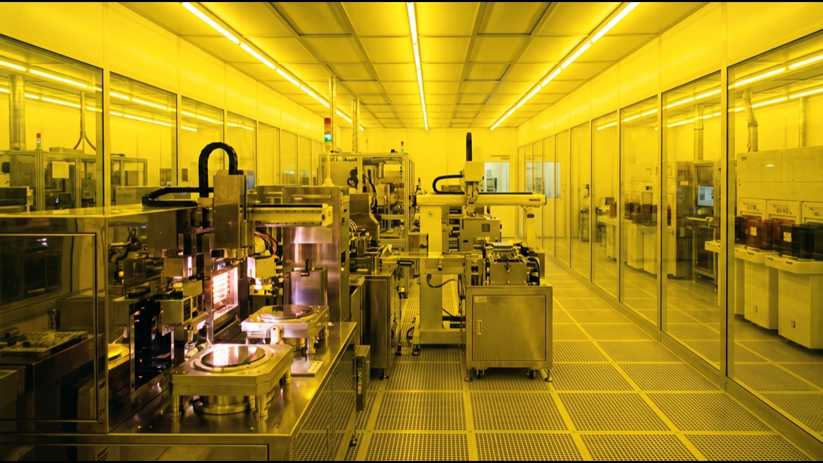
Chip features are so small that a single dust particle landing on a wafer mid-process can permanently ruin an entire chip, which is why fabrication plants operate cleanrooms with air quality thousands of times purer than a hospital operating theater.
Workers inside these cleanrooms wear full-body suits that cover essentially everything, and the air itself is continuously filtered and replaced at a rate designed to remove any stray particle before it has any realistic chance of settling on an exposed wafer surface.
How Ordinary Sand Becomes Ultra-Pure Silicon Wafers
Silicon, the second most abundant element in the earth's crust, is refined from quartz sand through a series of chemical purification steps until it reaches a purity level of roughly 99.9999999%, a standard far beyond what almost any other industrial material requires.
That purified silicon is melted and grown into a single continuous cylindrical crystal, which is then sliced into thin circular wafers and polished to a mirror finish smooth enough that any remaining surface irregularity would interfere with the microscopic patterns about to be printed onto it.
How Photolithography Actually Prints the Circuit Pattern
Photolithography works much like a highly precise photographic printing process, projecting light through a patterned mask onto a wafer coated with a light-sensitive chemical, transferring the circuit design onto the silicon surface with extraordinary fidelity.
Each chip requires dozens of separate lithography passes layered precisely on top of one another, since a modern processor's full circuit design cannot physically be printed in a single exposure and must instead be built up gradually, layer by painstaking layer.
Why Extreme Ultraviolet Light Became Genuinely Necessary
As transistor features shrank below what older lithography light wavelengths could physically resolve with adequate precision, the industry was forced to adopt extreme ultraviolet light, a wavelength so short that it is absorbed by virtually everything, including ordinary air itself.
Generating and focusing this extreme ultraviolet light reliably at industrial scale required one of the most complex machines ever engineered, a single unit costing well over one hundred million dollars and produced by essentially only one company worldwide capable of building it.
How Etching Actually Carves the Patterned Design Into Silicon
After the light-sensitive coating is exposed and developed, exposing the intended pattern, an etching process uses reactive chemicals or plasma to remove material precisely from the unprotected areas, physically carving the circuit pattern into the underlying silicon layer.
Etching must be controlled with extraordinary precision in both depth and direction, since even a minuscule deviation at this stage can distort transistor dimensions enough to change how the finished device actually performs electrically.
How Doping Actually Changes Silicon's Electrical Properties
Pure silicon on its own is a relatively poor conductor of electricity, so manufacturers introduce tiny controlled amounts of other elements into specific regions of the wafer, a process called doping, which deliberately alters how easily electrons move through that particular region.
Precisely controlling which regions are doped, with which element, and at what concentration is what allows engineers to create the specific electrical behavior that makes a functioning transistor possible in the first place, rather than just a uniform slab of semiconductor material.
How Multiple Layers Are Actually Stacked to Build Complete Transistors
A finished modern chip is not built in a single flat plane but as a genuinely three-dimensional structure, with dozens of distinct layers of transistors, insulation, and metal wiring stacked precisely on top of one another to connect billions of individual components.
Each additional layer must align with sub-nanometer precision to every layer beneath it, since even a minute misalignment between layers can break the electrical connections the entire chip depends on to function correctly.
Why Modern Transistors Are Measured in Nanometers
Chipmakers describe their manufacturing capability using a process node number measured in nanometers, historically corresponding to a specific transistor feature size, though modern node names have become more of a marketing convention than a literal physical measurement.
Smaller nodes generally pack more transistors into the same physical area, which typically improves performance and power efficiency, which is precisely why leading manufacturers invest enormous sums racing to shrink their process nodes ahead of competitors.
How a Single Fabrication Plant Actually Costs Billions of Dollars
A cutting-edge semiconductor fabrication plant, commonly called a fab, can cost anywhere from ten to twenty billion dollars to build, driven overwhelmingly by the cost of the specialized manufacturing equipment installed inside rather than the building's physical construction itself.
A single extreme ultraviolet lithography machine alone can cost well over a hundred million dollars, and a modern fab requires dozens of different categories of similarly expensive specialized equipment working in precise coordination to complete the full manufacturing process.
Why Only a Handful of Companies Can Make Cutting-Edge Chips
The staggering capital cost, combined with the deep engineering expertise required to operate at the leading edge, has consolidated the most advanced chip manufacturing into just a small number of companies worldwide, a dramatic contraction from dozens of competitive fabs decades earlier.
This concentration has become a genuine geopolitical concern for many governments, since a disruption at any single one of these few facilities could meaningfully affect global supply of the most advanced chips underlying modern electronics, defense systems, and artificial intelligence infrastructure.
How Chips Are Actually Tested Before Ever Leaving the Fab
Before a wafer leaves the fab, every individual chip on it is electrically probed and tested while still attached to the wafer, allowing manufacturers to identify and mark defective chips before investing further cost in cutting and packaging them.
This wafer-level testing catches the large majority of manufacturing defects early, since detecting a flaw at this stage is dramatically cheaper than discovering it only after a chip has already been packaged and installed into a finished device.
How a Finished Wafer Is Actually Cut Into Individual Chips
Once testing is complete, a precision saw or laser cutting tool slices the wafer along predetermined lines into individual rectangular chips, commonly called dies, a process that must be exact enough to avoid cracking the extremely brittle silicon material.
A single wafer can yield anywhere from dozens to many thousands of individual chips depending on how large each chip's design is, with larger, more complex chips naturally yielding fewer usable dies per wafer than smaller, simpler ones.
How Chips Are Actually Packaged After Being Cut From the Wafer
A bare silicon die is far too fragile and electrically exposed to be used directly, so it is packaged inside a protective casing that includes the tiny metal connections linking the chip's internal circuitry to the larger device it will eventually be soldered into.
Packaging technology has become an increasingly active area of innovation in its own right, with techniques that stack multiple separate chips together inside a single package now allowing manufacturers to combine specialized components more efficiently than building everything onto one single monolithic chip.
Why Yield Rate Is the Industry's Most Closely Guarded Metric
Yield rate, the percentage of chips on a wafer that function correctly after manufacturing, directly determines a fab's profitability, since the enormous fixed cost of running the facility remains essentially the same whether yield is high or disappointingly low.
Manufacturers treat their exact yield figures as closely guarded trade secrets, since a competitor with insight into low yield on a new process node could reasonably infer manufacturing difficulties or lower profitability than that manufacturer wishes to publicly reveal.
How Design Files Actually Travel From Engineers to the Fab
Chip designers work in specialized software that lays out the exact position of every transistor and wire, ultimately producing an extraordinarily detailed digital blueprint that is transmitted to the fabrication plant to generate the physical photomasks used in lithography.
This handoff between design and manufacturing requires extremely close technical coordination, since a design that looks correct on screen can still fail in physical manufacturing if it does not account for the fab's specific real-world process limitations and tolerances.
Why Taiwan Became the Center of Global Chip Manufacturing
Taiwan's dominant position in advanced chip manufacturing today traces back to a deliberate government-backed strategy launched decades ago to build deep domestic semiconductor expertise, combined with sustained private investment that compounded into a durable and difficult-to-replicate manufacturing advantage over time.
That concentration has made Taiwan simultaneously one of the most economically important places on the planet for the global technology industry and a genuine focal point of geopolitical tension, given how much of the world's advanced chip supply currently depends on facilities located there.
How Export Controls Have Genuinely Reshaped the Chip Industry
Several governments have imposed export restrictions on the most advanced chipmaking equipment and the resulting chips themselves, specifically aiming to slow other countries' ability to independently develop cutting-edge semiconductor manufacturing or advanced artificial intelligence capability.
These restrictions have measurably reshaped global supply chains and accelerated some countries' efforts to build independent domestic chip manufacturing capacity, though replicating decades of accumulated manufacturing expertise and specialized equipment supply chains genuinely takes many years even with substantial government support.
How Chip Shortages Actually Ripple Through Global Supply Chains
A modern car can require more than a thousand individual chips, and a shortage of even one relatively simple and inexpensive chip type can halt an entire vehicle assembly line, since the finished product cannot ship without every single required component present.
The widely reported chip shortage of the early 2020s demonstrated just how tightly global manufacturing has become interconnected, as a production disruption originating at a single facility rippled outward to affect car manufacturers, appliance makers, and electronics companies across entirely different industries worldwide.
What Makes Building a Brand New Fab So Genuinely Slow
Constructing a new leading-edge fab typically takes several years from initial groundbreaking to actual production output, a timeline driven by the sheer complexity of the specialized equipment installation, extensive process qualification testing, and the deep technical training required for the specialized workforce.
Even after physical construction is complete, a new fab must pass through a lengthy process of tuning its manufacturing steps to achieve commercially viable yield rates, a process that alone can take a year or more of continuous refinement before mass production truly begins.
How Surging AI Chip Demand Is Reshaping Fab Investment
The rapid growth in demand for specialized chips used to train and run artificial intelligence models has driven an unprecedented wave of new fab investment commitments worldwide, as manufacturers race to secure enough future capacity for what many expect to be sustained multi-year demand growth.
This surge has also intensified competition for the specialized manufacturing equipment itself, since the machines required to build these advanced chips are produced by only a handful of suppliers worldwide who cannot instantly scale their own production to match every customer's accelerating timeline.
What the Next Generation of Chipmaking Technology Looks Like
Manufacturers are actively pursuing new transistor architectures that stack components more efficiently in three dimensions, aiming to keep improving performance and efficiency even as the physical limits of further simply shrinking transistor size come increasingly into view.
Parallel research into entirely new materials beyond traditional silicon, along with radically new chip packaging techniques that combine multiple specialized chips more efficiently, represents the industry's broader bet on how meaningful improvement can continue once conventional transistor scaling eventually reaches its physical limits.
How Memory Fabs Actually Differ From Logic Chip Fabs
Although both rely on the same underlying lithography, etching, and doping principles, memory fabs optimize their processes to repeat the same simple cell billions of times at maximum density, while logic fabs optimize for a far greater variety of different specialized transistor designs.
This difference in priority means a leader in memory manufacturing is not automatically capable of competing in logic manufacturing without significant additional investment, which is why most major companies have historically specialized primarily in one category rather than the other.
How the Fab's Supply of Ultra-Pure Chemicals and Gases Is Managed
A chip fab consumes enormous quantities of ultra-pure chemicals and gases that must be supplied continuously without interruption, since even a very minor contamination in a single supply can ruin entire production batches worth millions of dollars before the problem is even detected.
This requires highly specialized suppliers subject to extremely strict quality auditing, and recent supply chain disruptions affecting these critical materials have pushed several fabs to diversify their suppliers or maintain considerably larger backup inventory than they traditionally kept in the past.
How the Specialized Workforce Needed to Run a Modern Fab Is Trained
Operating advanced chip manufacturing equipment requires technicians and engineers trained to an extremely high degree in precision techniques found in almost no other industry, meaning building an adequate workforce takes years of specialized training even after the physical building itself is complete.
Major manufacturers invest heavily in internal training programs and dedicated university partnerships specifically to supply a pipeline of qualified future employees, a long-term investment reflecting the genuine global scarcity of these highly specialized skills relative to growing demand from newly constructed fabs.
How Government Subsidies Are Shaping New Domestic Fab Construction
Several governments worldwide have launched large financial support programs offering grants, tax breaks, and subsidized loans specifically to encourage major chip manufacturers to build new facilities on their own soil rather than relying entirely on existing facilities located elsewhere in the world.
These programs reflect growing national strategic concern about excessive dependence on a geographically limited concentration of advanced chip manufacturing, though critics note that financial support alone cannot fully substitute for the decades of accumulated manufacturing expertise genuinely required to achieve commercial success.
Sources
- Wikipedia — overview of semiconductor manufacturing processes and technology
- Semiconductor Industry Association — industry data on chip manufacturing capacity and supply chains
- National Institute of Standards and Technology — technical standards and research on semiconductor manufacturing
- U.S. Department of Commerce — policy data on semiconductor export controls and industry investment
- International Monetary Fund — economic analysis of global semiconductor supply chain concentration
FAQ
Why does chip manufacturing require such extreme cleanliness?
Chip features are so microscopically small that a single dust particle landing on a wafer can permanently destroy a chip, so fabs use cleanrooms far cleaner than a hospital operating room.
Why does a new fab cost tens of billions of dollars?
The cost is dominated by dozens of categories of extremely specialized manufacturing equipment, including lithography machines that alone can cost over a hundred million dollars each.
Why can only a few companies make the most advanced chips?
The enormous capital cost combined with decades of accumulated manufacturing expertise has consolidated leading-edge production into a small number of companies worldwide.
How does a small chip shortage disrupt an entire industry?
A modern product like a car can require over a thousand different chips, and missing even one inexpensive type can halt final assembly since every required component must be present to ship.
Why did Taiwan become so central to global chip manufacturing?
Decades of deliberate government-backed investment in semiconductor expertise compounded into a durable manufacturing advantage that has proven very difficult for other countries to replicate quickly.
About the Author
We reference Wikipedia, Semiconductor Industry Association, National Institute of Standards and Technology, U.S. Department of Commerce, and International Monetary Fund to explain the background and current understanding of this topic.
Loved This Article?
Share it on WhatsApp → Share it on WhatsApp
Get more guides in your inbox — Subscribe to our newsletter for weekly surprising stories from Egypt, Saudi Arabia, Dubai, and beyond.